Etching
Etching is a technique to create patterns in glass and silicon substrates by chemically or physically removing selected parts from the surface of the wafer. The removal of material can be limited to a specific layer, but can also consist of a larger portion of material. Etching can be performed using wet or dry techniques, depending on the substrate material and the desired geometry of the etched structure. In wet etching, liquid chemicals are used, where dry etching makes use of gases or plasmas as etchants. Powder blasting is another etching method for silicon and glass patterning.
Wet etching
Micronit applies wet chemical etching techniques to create structures in glass and silicon. For glass, hydrofluoric acid (HF) is used as an etchant, which produces an isotropic etch profile. In addition to etching glass and silicon, Micronit offers the etching of various thin film metals such as Au, Cr, Cu, Ni, Ti and the etching of non-conductors such as oxide and nitride.
As with dry etching, the pattern is defined using photolithography. The structures that are created can be positioned with an accuracy within one µm. Masks are used to define the shape of the structure.
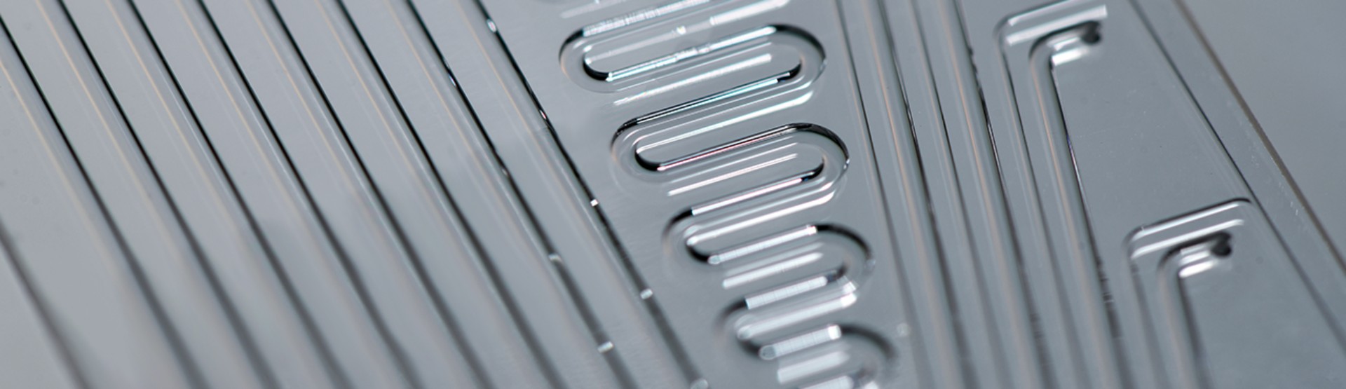
Isotropic wet etching (glass)
In wet etching of glass, hydrofluoric acid (HF) is the liquid etching agent. This technique is isotropic: the glass dissolves in all directions equally fast. As a rule, in isotropic etching, channel width = the initial mask opening plus twice the etch depth. Besides, the corners of the channel are rounded. The surface of the etched structures is, corresponding to the type of glass used, very smooth.
Anisotropic wet etching (silicon)
Anisotropic etching of silicon is done using alkali hydroxides such as KOH, NaOH, or amine-containing solutions such as TMAH. KOH is the most popular, having been in industrial use for decades. Because silicon is a monocrystalline material, etching of the crystal planes always yields the same etching angle. By making use of the varying etch rates of the different crystal planes, the desired geometry of the structure can be achieved. Already during the production of the wafer it is determined which angle on the crystal lattice is required to obtain the needed structure. Depending on the temperature and concentration, various etch rates and surface roughnesses can be achieved. Masking is generally done using a nitride layer, which is typically patterned using photolithography followed by RIE.

Why work with us?
At Micronit, we specialize in accompanying our customers all the way from idea to production. Are you looking for a development and manufacturing partner? Take a look at our route to success!
Is your project in need of a wet etching solution? Please contact our experts!