Wafer bonding is a key technology in the fabrication process of lab-on-a-chip devices. Especially now microfluidic devices gain in on-chip complexity, only the most advanced bonding techniques can meet the requirements. In particular systems that are used in biological, pharmaceutical, or medical applications, require newly developed bonding methods that leave the sensitive biological material undamaged during the process.
Micronit is experienced in the bonding of polymer, glass, silicon, and hybrid devices and can offer customer-specific bonding solutions when needed. We provide solutions for the integration of porous membranes, flexible films, sensors, and biosensors as well as for assembly, sealing, packaging, and labeling of lab-on-a-chip devices.
Temperature-dependent bonding technologies
Temperature is an important factor in determining which bonding process to use. Bonding at low temperatures is necessary when dealing with devices that contain temperature-sensitive elements, like certain coatings, polymers, or biological materials.
In a product development process, we will always discuss the specific bonding requirements of the product with our customers. Overseeing the entire manufacturing process and considering costs and scalability, the right choices in materials and processes can be made.
Wafer bonding techniques
There are different wafer bonding techniques, each having their own advantages and restrictions.
-
Direct/fusion bonding
-
Anodic bonding
-
Eutectic bonding
-
Adhesive bonding
-
Laser-assisted room temperature bonding
Direct/fusion bonding
Fusion or direct bonding is a technique that joins two or more wafers of the same material. A direct bond is typically annealed at a high temperature, which makes the bond as strong as the mechanical strength of the base material. However, annealing a direct bond at lower temperatures is also feasible. In direct bonding, it is essential that the surface quality (smoothness) of both wafers is extremely high.
Anodic bonding
Anodic bonding is a technique that allows two or more wafers of different materials (silicon and borosilicate glass) to be bonded. The process of anodic bonding is usually done at about 400°C, which is a lower temperature than typical temperatures used for direct bonding. The lower temperature reduces the tension in glass and silicon layers. Compared to direct bonding, anodic bonding places slightly less demands on the surface quality of the material to be bonded.
Eutectic bonding
Eutectic bonding is based on the ability of silicon to form a eutectic alloy with certain metals. Through the application of pressure and heightened temperatures, a permanent bond is forged between two wafers, facilitated by a thin metal layer. An established eutectic alloy is gold-silicon.
Adhesive bonding
In adhesive bonding, substrates of different types of materials (e.g. silicon, glass, metals and other semiconductor materials) are connected by an intermediate layer. The intermediate adhesive layer can be a type of glue, or for instance, a photo-patternable dry film resist/adhesive. Bonding temperatures depend on the material of the bonding partners and on the type of intermediate layer, but are typically lower than in other bonding methods. Bonds can be hermetic or not, depending on the type of adhesive used.
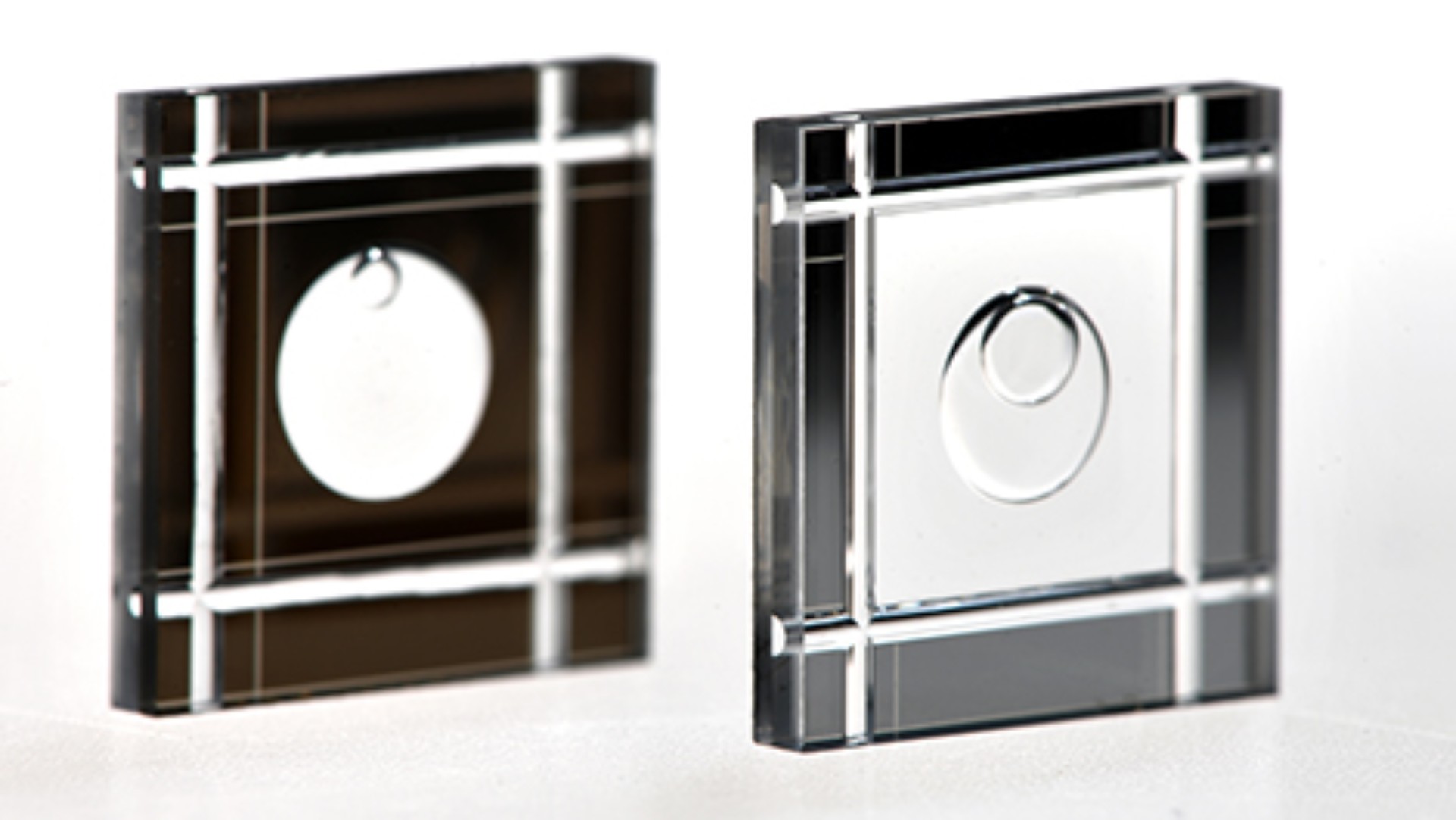
Laser-assisted room temperature bonding
Micronit has developed this patented bonding process that can generate hermetic bonds, while only locally applying heat. Substrates can be of glass or silicon, or a hybrid combination of both. In this technique, first, a prebond is made using a metal interlayer. After this, the formed prebond is locally strengthened by laser processing. Because the heat-affected zone is very limited, temperature-sensitive components, like biomaterials or liquids, can be part of the bonded stack.
Micronit offers a broad range of bonding capabilities so that requirements for hybrid integration and specific applications or materials can be met.
Are you looking for some more detailed info on our bonding capabilities? We have an application note on this topic.
