(Deep) Reactive Ion Etching (D)RIE

Dry etching of silicon-glass hybrid products


Silicon-glass hybrid chips typically compose of a silicon layer which contains dry etched structures, bonded with a plain or structured glass layer. Anodic bonding creates hermetically sealed chips without the use of adhesives or intermediate layers. The glass layer is fully transparent, while the silicon layer is not transparent for visible light (only for infrared).


Usually hybrid chips consist of a crystalline silicon layer combined with:

  • BF33 glass

  • MEMPax glass

Benefits of hybrid chips

  • Bonding is done without additives (anodic): no autofluorescence or compatibility issues

  • Optical transparency on one side (glass-si)

  • Optical transparency on both the top and bottom when using a triple stack (glass-si-glass)

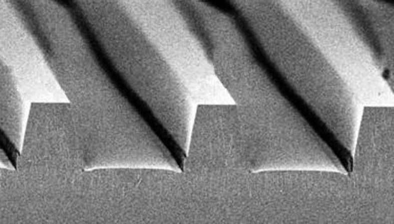
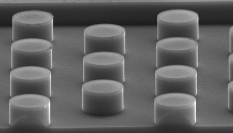
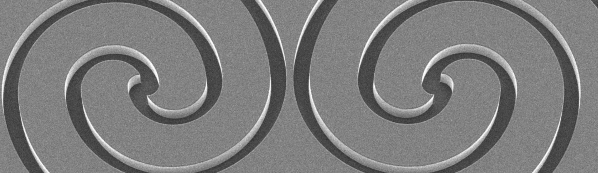
In hybrid chips, the action usually takes place on the silicon layer, where the relevant structures are applied. This can be a system of microfluidic channels or, for example, a pillar structure. The most commonly used etching methods to create these structures are Reactive Ion Etching (RIE) and Deep Reactive Ion Etching (DRIE).

Silicon etching

Reactive ion etching (RIE) is a specific etching technique, typically used when high aspect ratio structuring is required. RIE can generate deep structures and steep side walls: ultimate examples of anisotropic etching. But it can also be used to produce through silicon vias (TSV’s).


RIE is a dry etching process, performed with gases. Along the process, the gas molecules are broken up into ions, which bombard the surface of the wafer or substrate to create the desired structure.


At Micronit, we specialize in Deep Reactive Ion Etching (DRIE), using the Bosch process. This process consists of alternating etching and passivation steps. This cycle of steps is repeated just as long as it takes to reach the desired etch depth or through hole.

Benefits of RIE/DRIE

  • Large design freedom:

    • aspect ratios up to 1:50 (width versus height) are within reach

    • walls are not curved but straight

    • angles closely approach 90°, usually with a slight taper of 1-3 degrees

  • Very smooth channel walls

  • Highly accurate structures

  • Good chemical compatibility

Channel structures in glass

Things to consider in using RIE/DRIE

  • Inlet holes can be both positioned in the glass or the silicon layer.

  • When wall shape and roughness are critical, this can be tuned by process optimization.

  • When structures with large differences in dimensions are combined on a single wafer, this might require some additional attention and optimization.

  • When using a triple stack (glass-si-glass), there is the option to create a product with silicon-only sidewalls. Both the top and bottom layers are glass, with a thin silicon layer (typically 2-250 µm) in the middle.

    • For the specialists: the silicon layer placed between the two glass layers is the device layer of a SOI wafer. The device layer of the SOI wafer is structured using DRIE etching. After that, the total SOI wafer is bonded to a glass layer and then the carrier layer of the SOI wafer is removed. Subsequently, the additional glass layer is bonded to the stack.

Other options

Dry etching tends to be more expensive than wet etching, so for profitability reasons it can be good to weigh your options. Also if you prefer a full glass product (for optical quality reasons perhaps), this has consequences for the etching possibilities.

Alternative routes to consider:

  • Wet etching of glass (glass-glass chips)

    • Isotropic etch process: consider the design restrictions.

  • Dry etching of glass (glass-glass chips)

    • Limited design freedom: maximum structure depths of 20µm.

Product examples

At Micronit, we have used our dry etching capabilities for various projects.

DLD chips

We have created silicon-glass chips with a structure of hundreds of tiny pillars, which are used for deterministic lateral displacement (DLD). DLD is a microfluidic cell sorting technique that utilizes an asymmetrical array of pillars to separate particles. The structuring is done on the silicon layer that is bonded to a glass layer.

Pillars in silicon, fabricated using DRIE

EOR chips

A triple stack (glass-si-glass) can be found in certain enhanced oil recovery (EOR) chips, that have a middle silicon layer that simulates the structure of physical rock.

Enhanced oil recovery chip, structured using DRIE - photo’s courtesy of TU Clausthal

In need of advice?

Micronit specializes in dry etching techniques, both as a separate processing step and as part of a total product development process. Contact us to discuss your requirements with our experts!